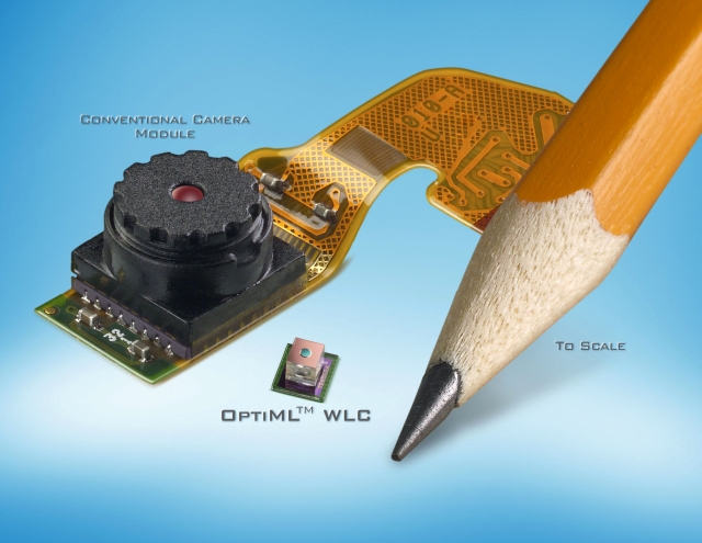
In a press release earlier this year, Tessera (TSRA) announced a new technology for making extremely small and lower cost camera modules for devices such as camera phones, webcams and security cameras. The size reduction possible with the new technology Tessera calls OptiML™ Wafer Level Camera Technology is impressive as shown in the illustration below.
This reduction in camera size will enable designers of mobile phones and other portable products to fashion still more compact devices. The design of earlier products, particularly the thickness, has often been dictated by the height of the included camera module. Using Tessera’s technology, product designers will be free to incorporate cameras in extremely thin new designs. The reduced size and cost of camera modules will also enable designers to place cameras in entirely new product categories.As with many prior technologies, when cost and size are reduced adequately, the technology proliferates and becomes ubiquitous, leading to large market opportunities. By making its camera technology available through licensing to the industry, Tessera means to profit as manufacturers roll out new modules, and industrial and consumer products based on OptiML™ Wafer Level Camera Technology. Perhaps the first instance of the new Tessera technology going to market is the recent licensing agreement with Toshiba.
As we look ahead to the new year we will watch for further licensing deals, design-ins and products incorporating this and other steadily evolving optoelectronic technologies.


0 comments:
Post a Comment